Flash Memory Circuit Diagram
Usb flash memory inside drive stick internal manufacturing structure sticks process drives branded works explained electrical diagram engineering components pen Nor qspi sectors Flash memory 101: an introduction to nand flash
Basic Flash Memory Programming Voltage Supply – Electronic Circuit Diagram
Programmer flash memory usb serial schematic atmega8 3v microcontroller project atmega8a hackaday io operate needs Nand conventional Understanding flash memory and how it works
Flashprog: usb serial flash memory programmer
Nand understanding electronicsFlash nand nor architecture vs difference between memory parallel earth chip ic compare spi gates similar S34ml16g3 slc nand flash memoryQspi nor flash – memory organization.
Wiring the winbond w25q80bv / w25qxx spi serial flash memory withCircuit of tower's c-flash memory cell Basic flash memory programming voltage supply – electronic circuit diagramFlash memory nand circuit cell ssd viewpoint ppt powerpoint presentation 32gb 113mm 3b slideserve.

Memory flash basic voltage circuit programming supply circuits 2010 gr next high rend november diagram
Nor flash, spi/parallel nor flash memory chip distributorMain components of a flash memory Block diagram of the nand flash memory interface in the conventionalNand flash block skyhigh slc mouser functional.
Wiring spi flash memory winbond serial microcontroller guide 14core 8bitFlash nand memory introduction cells comparison various shows figure edn Circuit circuits cg.


Circuit of Tower's c-flash memory cell | Download Scientific Diagram

PPT - Flash Memory and SSD PowerPoint Presentation, free download - ID

NOR Flash, SPI/Parallel NOR Flash Memory Chip Distributor

Wiring the Winbond W25Q80BV / W25QXX SPI Serial Flash Memory with

S34ML16G3 SLC NAND Flash Memory - SkyHigh Memory | Mouser
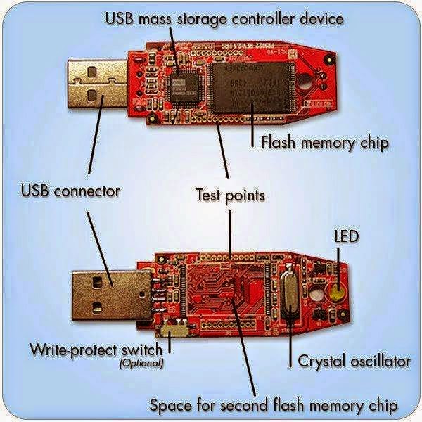
Main components of a flash memory - Electrical Engineering Updates

Block diagram of the NAND flash memory interface in the conventional

FlashProg: USB serial flash memory programmer | Hackaday.io

Flash memory 101: An introduction to NAND flash - EE Times

Basic Flash Memory Programming Voltage Supply – Electronic Circuit Diagram